


Mysuru Builds Future: New Tech Park Makes City Top Spot for Computer Boards Mysuru is quickly becoming a major center for making computer circuit boards, as a big new tech park begins operations right now. This essential move places Mysuru at the heart of producing essential parts found in all computers, mobile phones. internet devices around the world. The new hub means many new jobs and a strong push for making more technology inside the country, showing a big step forward in India’s own manufacturing story. This development firmly establishes the city as a critical player in global electronics.
A New Start for Industry in Mysuru
Mysuru, a city known for its rich history and cultural importance, is now set to become a major hub for making electronic parts. This big change comes with the planning and building of a new technology park. This park will focus on the creation of Printed Circuit Boards, often called PCBs. These boards are the very basic building blocks of almost all electronic devices we use every day. From the computer we work on, to the mobile phone in our pocket. even the car we drive, PCBs are inside them all, allowing the different parts to talk to each other and work correctly.
The move to make Mysuru a center for PCB manufacturing is a big step for the region. It shows a clear plan to bring more modern industry and jobs to the area. For many years, Mysuru has been a place of learning and tourism. Now, it is also stepping into the world of high-tech manufacturing. This change is expected to bring new skills and opportunities for many people.
“Our goal is to make Mysuru a key player in the global electronics supply chain,” said a government spokesperson recently. “This new technology park is a big part of that plan. It will help us build a strong base for manufacturing and bring in new kinds of jobs for our people. We believe this will make Mysuru a very essential city for technology in the years to come.”
The government and local leaders have been working together to make this dream come true. They see the need for India to make more of its own electronic parts instead of buying them from other countries. By building this park, Mysuru will play a big role in making India stronger in the world of technology.
Why This Place?
Mysuru was chosen for this big project for several good reasons. First, the city has good connections to major roads and cities. This makes it easy to move materials in and finished products out. Second, Mysuru already has some essential technology companies and colleges that teach engineering and computer skills. This means there is a good number of people who already have some of the skills needed for a high-tech park.
The city also has a stable power supply and enough land available for big industrial projects. These are very crucial for any large manufacturing plant. Also, the cost of setting up a business and living in Mysuru is generally lower compared to bigger cities. This can make it more attractive for companies looking to start new operations.
Local leaders also believe that Mysuru’s calm environment and good quality of life can help attract skilled workers from other places. They see it as a place where people can work in advanced industries and also live well with their families. This mix of good location, available land, skilled people. a good living environment makes Mysuru a strong choice for a big technology park focused on PCB manufacturing.
What the Park Will Do
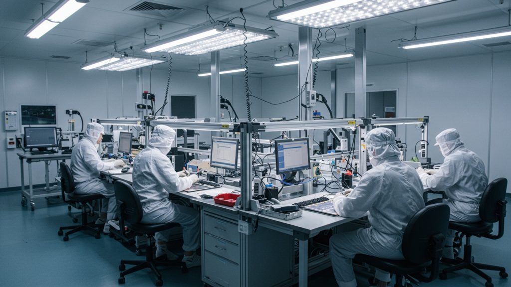
The new technology park in Mysuru will be a large area specially designed for companies that make PCBs. It will have all the special buildings and tools needed for this type of work. This includes clean rooms, where very tiny electronic parts can be put together without dust or dirt getting in. It will also have advanced machines for making the circuit paths on the boards and for putting all the small parts onto them.
The park will not just be for making PCBs. It will also be a place where new ideas are created. There will be special centers for research and development. This means scientists and engineers will work on making PCBs even better and finding new ways to use them. This focus on new ideas is essential for the park to stay modern and competitive in the fast-moving world of electronics.
The park will also have shared facilities that all companies can use. This might include testing labs, power stations. waste treatment plants. Sharing these resources can help reduce costs for the companies operating inside the park. The aim is to create a complete environment where PCB manufacturing can happen smoothly, from start to finish. Companies that make different parts of the PCB, or design them, can all be in the same place, making it easier to work together.
Jobs and Money
Building this new technology park and bringing in PCB manufacturing companies will have a big impact on jobs and the local economy. It is expected to create many direct jobs within the park itself. These jobs will range from skilled engineers and technicians who operate the complex machines, to workers who help with assembly and quality control. There will also be jobs for people who manage the factories and work in administrative roles.
Beyond the direct jobs, many more indirect jobs will be created in Mysuru and the surrounding areas. For example, there will be more demand for housing, food services, transport. other local businesses that support the people working at the park. This will mean more money flowing into the local economy, helping many different kinds of businesses to grow.
The project is also expected to attract significant investment from companies both inside and outside the country. When big companies decide to set up factories in Mysuru, they bring in large sums of money. This money is used to build the factories, buy machines. pay salaries. This kind of investment is vital for the long-term growth of the region. Local government figures suggest the impact will be substantial:
| Area of Impact | Estimated Benefit (First 5 Years) |
|---|---|
| Direct Jobs Created | Over 7,000 |
| Indirect Jobs Created | Over 15,000 |
| Total Investment Attracted | Billions of rupees |
| Boost to Local Economy | Significant increase in regional product |
This economic boost will help improve living standards and provide more opportunities for the people of Mysuru and the entire region. It is a step towards making the area a center for advanced manufacturing and a contributor to the nation’s technology goals.
Who is Helping Make This Happen?
Many essential groups are working together to make this new technology park a reality. The state government is playing a central role. They are providing the land, helping with the necessary approvals. offering support to companies that choose to set up their units in the park. Their policies are designed to make it easy and attractive for businesses to invest in Mysuru. They see this project as a key part of their plan to grow the state’s economy and create jobs.
Industry bodies, which represent various companies in the electronics sector, are also actively involved. They are giving advice on what kind of facilities are needed and what challenges companies might face. Their experience is very essential to make sure the park meets the actual needs of PCB manufacturers. They also help spread the word about the opportunities in Mysuru to their member companies, encouraging them to consider setting up operations there.
“The partnership between the government and the electronics industry is strong,” explained a representative from a leading industry association. “We are all working towards a common goal: to make India self-reliant in electronics manufacturing. Mysuru’s new park is a perfect example of how this can be achieved when everyone works together.”
Local authorities in Mysuru are also key partners. They are responsible for making sure the area has good roads, water. other basic services needed for such a large industrial project. They also work with the community to make sure people comprehend the benefits of the park and how it will help the city grow. Educational institutions, like colleges and technical schools, will also play a role by training students with the right skills needed for jobs in the PCB manufacturing industry. This cooperation among different groups is what will ensure the success of the new technology park.
Looking Ahead
The journey to become a major PCB manufacturing hub is a long-term plan for Mysuru. The first steps involve getting the basic infrastructure ready at the new technology park. This means building roads, power lines. water systems. After that, companies will start to build their factories inside the park. This process will take some time. it will happen in different stages.
As more companies set up their operations, the park will grow in size and the number of jobs will increase. Over time, Mysuru is expected to become a place where not only PCBs are made. also where new ideas for electronic products are born. This could lead to more advanced manufacturing and research happening in the city.
The success of this park could also encourage other similar industries to look at Mysuru as a good place to set up their businesses. This could create a snowball effect, bringing even more technology and industry to the region. The vision is for Mysuru to be recognized globally as a strong center for electronics manufacturing, contributing significantly to the nation’s technological progress and economic strength. This initiative marks a new chapter for Mysuru, moving it towards a future deeply connected with advanced technology and industrial growth.
![]()
